Stefan Reber Photovoltaics
An opportunity for production in Europe
Why do you see this new production plant as an opportunity?
From a global perspective, photovoltaics is conquering all areas of energy provision. Photovoltaics is in many places already the cheapest way to produce usable energy, in this case electricity. We need terawatts of installed photovoltaic capacity worldwide. In Bitterfeld we plan to develop an annual production capacity of at least two to three gigawatts, in various stages. The world market today is 120 gigawatts. So we want and need to continue to scale up and expand in order to capture a significant share of the world market. We want to bring photovoltaics back to Europe and do our bit to drive forward the energy transition.
What is special about your method? Why could production be successful in Germany as well?
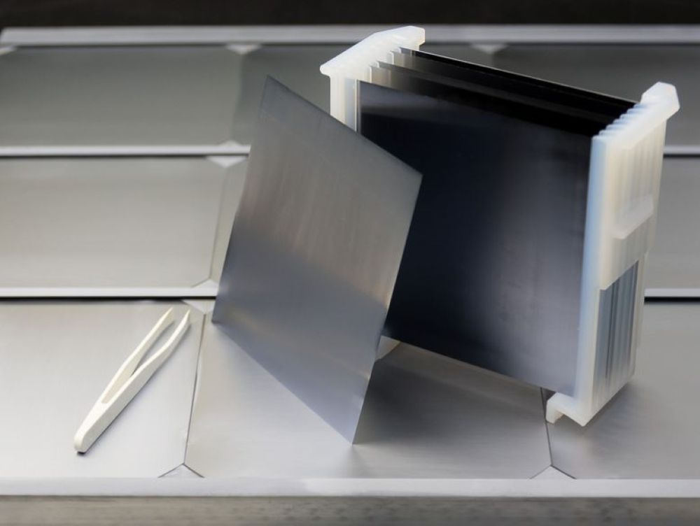
In a nutshell, I would say that we produce wafers and not waste. That's of course putting it very simply. The classic technology for producing high-quality monocrystalline wafers is called the Czochralski method. This involves producing high-purity silicon from the chemical chlorosilane, at high temperatures with a very high energy expenditure. This is then melted down, from which cylindrical crystal rods are drawn and which in turn are then squared. This means that a cuboid is cut from the round crystal, which in turn is cut into individual panes with wire saws. During the process a lot of silicon is more or less machined into useless waste and is then lost, despite great efforts to recycle it. So you could almost say it's a process to produce waste and wafers are a by-product.
And with you it's different?
Exactly, we do it completely differently. We start with the same raw material, chlorosilane, and we also end up with the same product, the silicon wafer - which, however, has better properties than the classic wafer and can therefore also achieve higher efficiencies. In between, we eliminate all process steps that consume a lot of energy and produce a lot of waste. We replace this with silicon epitaxy or silicon separation. And with this method we clone a classic wafer. This means that I take a wafer produced in the classic way, place a separation layer on top of it, then use the separation process to let a second wafer grow on this wafer, which I can remove in the next step.
How is it possible that the cloned wafer has exactly the same structure?
With the help of epitaxy. This is a growth process that copies, so to speak, the surface on which the growth starts. I have a gas phase in which the silicon atoms float. They will then find a good place to integrate themselves on the surface provided. And this place is typically a crystal lattice place. The new atom integrates itself into this regular lattice of the seed wafer's monocrystal. And then, atom by atom, naturally at high speed, a new layer grows.
The production process is the result of years of research and development, initially at the Fraunhofer Institute for Solar Energy Systems ISE, continued by NexWafe as a spin-off, in collaboration with Fraunhofer ISE. Over the years, the relevant federal ministries, most recently the BMWi, have supported this work. Which of the projects would you highlight?
When I joined Fraunhofer ISE in 1996, I was working on a BMBF-funded project called DüSi. The task was to develop crystalline silicon thin-film solar cells. Why do I bring this up? Because these projects laid the foundation for the separation technology and separation reactors that we use in NexWafe today. This means that we are building on more than 20 years of experience, which began at the ISE and other research institutes in Germany and around the world. A second project I would highlight is Si-CVD, which was started in 1999 at Fraunhofer ISE. A very important foundation was laid in the project, namely inline processing. This allows fully continuous production. One of the next major projects running at NexWafe and funded by the BMWi was EpiPower. Here we have made the step from the laboratory to pilot production.
What role does project funding play for you?
Without innovation we cannot survive in Germany and Europe. The competitive pressure from abroad is simply too high. But innovation also means risk. I don't know where the world is heading in three or four years. And this makes project funding an extremely important and essential part of minimising this risk to such an extent that the barrier is low enough to embark on an innovation.
What is the current status of the production plant in Bitterfeld? When is it going to be ready?
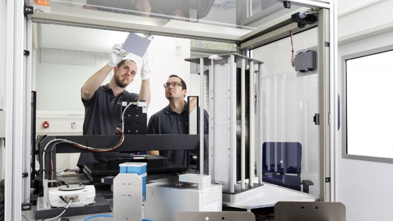
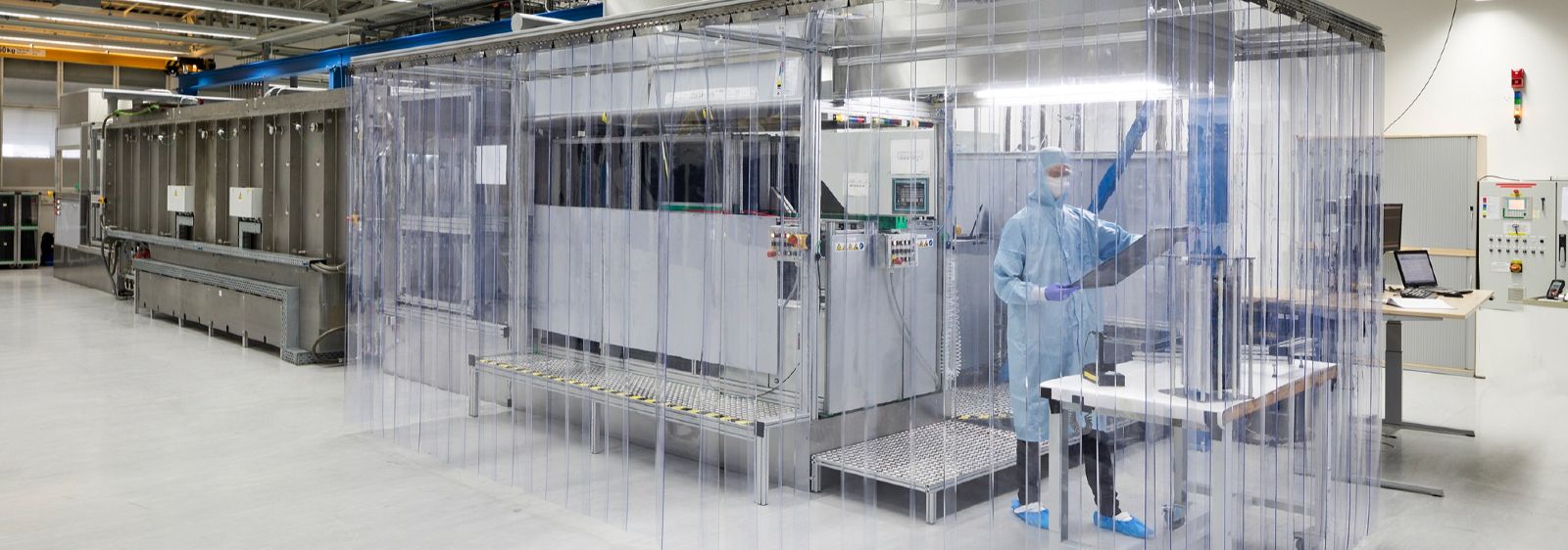
We're currently planning to commence construction in the first half of 2021. We will then need between nine and twelve months to build the epiwafer factory and integrate it into the existing infrastructure. Then the first wafer will come out of the factory in the first half of 2022. That's when mass production will really start.
Is NexWafe the only company that produces wafers in this way?
Other companies have also tried the kerfless production of wafers, but they have not managed to achieve the necessary throughput. In order to be able to produce photovoltaic quantities, we have to think in terms of one wafer per second, i.e. several thousand wafers per hour. This is why we focused very early on so-called inline production at ISE, from which we spun off. This is our core competence. And the other companies just don't have that. Besides us there is the US company 1366. It has a kerfless wafer method in which wafers are pulled out of the melt. This is also really exciting, but has the disadvantage that it can only be used to produce multicrystalline wafers - and that limits cell efficiency. The method does not manage to serve the currently dominant and emerging market of high-efficiency solar cells with 24 to 25 per cent efficiency - we can do it.
Is it fair to say that the goal has been achieved with the start of production?
This is the beginning. We have lots of ideas on how to develop and then also implement innovations based on this first product and many other product ideas.
What does it mean to you personally when kerfless wafer technology goes into mass production?
It makes me proud. I started at ISE in 1996, 24 years ago. As a doctoral student. During all this time, I have been more or less constantly working on the topic of silicon photovoltaics. That is to say, a large part of my working life has been invested in this. If we can get this to an intermediate stage where we can go into mass production and implement it, that means a lot to me.
What brought you as a scientist to the topic of photovoltaics?
A newspaper article by Martin Green in the late 80s. I was just finishing high school then. Martin Green said that with "buried-contact" solar cells we will be able to produce photovoltaics for 50 cents per watt in future. That was quite bold, because at that time one watt still cost 15 euros, which is a factor of 30. I ultimately found it so fascinating, also the theories of the Club of Rome, that I felt I had to be there. That is also what brought me to the ISE and that in turn brought me to silicon. As a physicist I found it very exciting to go into materials research, materials development. As I always say: Solar cells are fascinating. It still thrills me.
The interview was conducted by Meike Bierther, science journalist at Project Management Jülich.
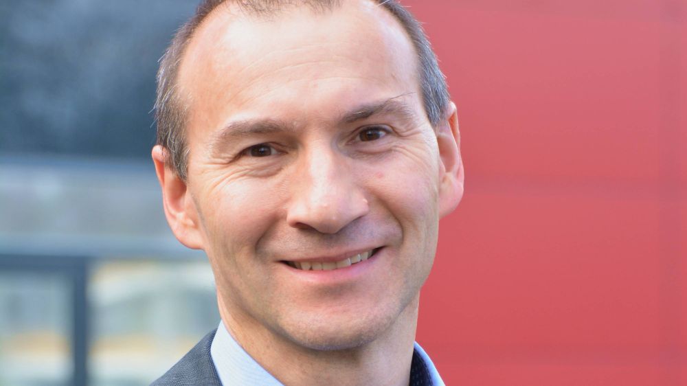
Dr Stefan Reber is managing director and co-founder of NexWafe GmbH, which was spun off from Fraunhofer ISE in 2015. In 1996 he started his scientific career at Fraunhofer ISE as a doctoral student and has been working with silicon ever since. During his time as head of department at Fraunhofer ISE, he already achieved numerous new developments and applied for several patents. He studied physics at the Technical University of Darmstadt and received his doctorate from the University of Mainz.

